Upgrading my BenEater inspired video card
Making the card useful

Last time I wrote about my video card, which was mostly the same as the one BenEater built in his excellent video series.
Over the holiday break in 2020, I wrote a little Nintendo Gameboy emulator for fun. Now seeing how the Gameboy worked, I was amazed by was how much they could do graphically with such restrictive hardware limitations - and it got me thinking: could I apply some of the same principles to make my video card actually useful?
The plan
The main problems with the existing card lie with the memory. There isn't enough, and it isn't fast enough. Switching out the EEPROM for RAM would not only fix the black lines caused by slow access time, but would also allow me to go for a larger amount of memory, since parallel access EEPROM is only available (as far as I know) up to 32kb (256k-bit). I would also be able to eliminate the repetition on the y-axis, and increase the colour depth to 8 bit (256 colours), with next to no changes in the overall design.
However, I would still have a problem to overcome in the long run, similar to what we saw in the third instalment of Ben's series - driving such a large amount of memory wouldn't be feasible for a relatively 'slow' CPU. I eventually want to hook this up to a home made computer, so I need the interface to be realistically drivable by a very simple computer.
This is where inspiration from the Gameboy design comes in. Instead of storing a byte (or nibble) for every pixel on screen, I could have some memory which contains pixel data for tiles, and some more memory defining which tile to draw at a given position on screen.
Phase 1 goals
- Expand colours from 16 (4 bit) to 256 (8 bit)
- Use full possible resolution with the 20Mhz clock (400x300*)
- Separate single EEPROM into 2, one for tiles, and one for the "map"
* Actually 800x600, but I'll only change colour every other pixel. 400x600 would be possible, but I'd like to maintain the 4:3 aspect ratio as it looks better
Emulating
First of all, to make sure this worked in theory, I wrote an emulator of my existing card. This helped a lot with ironing out problems, and served as an intermediary between idea and schematic.
I wrote the emulator in Typescript, because that's what I'm used to for work.


The first 3 bits of the horizontal (H) and vertical (V) would be used to select the pixel within the tile, then the output from the map memory would select which tile is being draw.
The map is addressed with the remaining H and V signals. The output of tile memory would be an 8 bit colour.
To achieve this I would need tile memory of 16kb and map memory of 4kb.
Here is how the emulation looked:

I already have some 32kb EEPROMs and since I paid for 32kb, I'm going to use all 32kb!
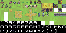
So I settled on 128 16x16 tiles, arranged like this:

That uses up all my memory, but gives me half as many tiles, because I can only use the first 7 bits of the map memory output before running out of address lines on the tile memory (more on this later).
My map memory is looking pretty pathetic too, only 1kb needed. This was all part of my cunning plan.
Planning for hardware scrolling
The Gameboy has a really cool feature in it's tile maps, which is that it allows you to have a map bigger than the screen. You can then move the "viewport" around without pushing new pixels or tiles to memory.
Here is a screenshot from my Gameboy emulator to demonstrate what I mean:

This would be the plan for my video card - real hardware scrolling! In my mind, since the card is mapping tiles and has 'hardware scrolling', that makes it a real GPU, because it's actually processing something. Therefore it's a GPU, not a video card so that is how I will refer to it henceforth.
The final memory map would look like this:

We don't yet have the extra H and V signals, but intend to implement them later, for now we'll just tie them to ground.
Here is an example tile set, and output of the emulation:

Breadboard prototype
If you read the first post I made, you'll know I already made the counter part of the card into a PCB, so I reused that

Since I already had the counter part of my GPU, I only needed to hook up the new memory map and colour decoding.
The memory hook up was simple - just a case of following the schematic I made and hooking up the right wires to the right pins on the memory.
The colour decoding was all new, but turned out to be pretty simple. At first I went down a rabbit hole looking for binary to analogue decoders, to turn the RGB binary output into voltages between 0-0.7v (required by VGA), but in the end, I just used resistors of different values just like the first card, only this time balanced the values for 3-bit outputs from the R and G signals, and 2 for B.
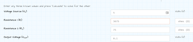
To figure out which resistor values I needed I did the following:
3-bit signal = 8 possible combinations / 8 output voltages: 0, 0.1, 0.2, 0.3, 0.4, 0.5, 0.6, and 0.7.
So 0b001 = 0.1v.
Which resistor value gives me 0.1v? I (lazily) plugged it into an online voltage divider calculator:
(note the monitor has a 75ohm resistor according to the VGA spec)
I repeated this for the 0b010 and 0b001 cases. In case you're not as lazy as I am, here is the actual formula:

I then checked my assumption that combinations of these resistors in parallel would give me my desired voltages (on another online calculator) and everything checked out.
I substituted them as needed for the closest values I had.

Here is the old colour palette:

And here is the new:
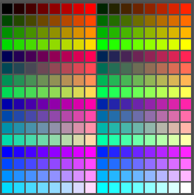
I had to tweak the resistors a little bit, because nothing ever works as well in real life as it does on paper. Probably has something to do with internal resistors in the EEPROM, or unwanted resistance in the wires - I will be more scientific about this later, but for now I just employed some trial and error.
Here is how the prototype came out:


EPROM side quest
I was actually very pleased with the results. It's a lot better than the original card, but I still have access time issues on the EEPROM. This is only temporary, as I plan to upgrade to SRAM, but I couldn't help but wonder if I would get any improvement if I switched to EPROM instead of EEPROM.
The EEPROM I have has an access time of about 150ns, but for a few pounds (pounds sterling, I'm British by the way) I could get some 70ns access time EPROM. Once I write to it, I can never erase it (as the missing E stands for erasable), but satisfying my curiosity was worth it.
Definitely an improvement, but 70ns still isn't fast enough when I'm clocking at 20Mhz (a pixel every 50ns), not to mention propagation delays.
Phase 2 goals
The plan to add hardware scrolling was exciting, but the black lines ruining the picture is taking some of the joy out of getting good results, so I decided to address this next.
The goals for the next phase would be:
- Swap (E)EPROM for SRAM
- Increase tile memory to 64kb since they make SRAM chips bigger than EEPROMs
- Build an interface so a computer can write to both memory chips
Swapping the EEPROM for SRAM
This was super easy, since the pin outs are basically the same (actually exactly the same for the map memory). For tile memory I upgraded and used that 8th bit from the map memory output I mentioned earlier. I couldn't find any 64kb RAM chips, so I ended up going for 128kb (1M-bit) - I'll just tie the last memory address bit to ground.
External interface
I've been dreading this for a while. I didn't want to copy Ben's solution for interfacing to his video card as it's quite tightly coupled to the particular computer he was using, and it was massively restrictive in terms of performance.
One good thing about my design is that once you've set up the tiles and map (via some kind of start-up routine), there won't be much additional writing required. You might change some tiles in the map, but you won't likely be pushing tonnes of data frequently.
My idea was to simply buffer the lines coming in from the counter, and out of the colour decoder, and turn them off when you want to write to the RAM. This would isolate the RAM allowing the computer to do with it as it pleases.
The screen will simply go black while things are loaded in, but after that there will be minimum disruption to the picture, since you can just write to RAM during blanking. I'll implement some kind of interrupt for the v blank later, and that time can easily be used to move the tiles around, but that's a problem for future Matt.
The design works something like this:

The interface consists of 2 8 bit inputs - DATA and WRITE_SELECT (WS)
WS allows you to disable the "draw" (0b00000001) which will stop the H and V signals from going to memory, and will disable output from the memory chips.
Then you can select to enable the write pin on the map memory, tile memory, or memory address registers (and some others, which haven't been designed yet)
The memory address registers (MAR) are new - they're simply 8 bit registers which are wired to the upper and lower bytes of both map and tile memory

The DATA bits are bussed to the MAR and (via a buffer to avoid interfering when drawing) to the IO lines of the memory.
As an example, here is what a computer would have to do to write to memory:


Almost immediately after ordering I realised I forgot to swap the map EEPROM for SRAM. I assumed it didn't matter much, because the pinout is the same, however I didn't realise that the only SRAM I had / could get hold of, was narrower than the EEPROM.
I may be able to get away with using EEPROM for the map, since it in theory will be accessed much less often than the tiles, but just in case I made a hacky adaptor for the SRAM while waiting for the boards to arrive.

A fruitful side quest - optimising the counter circuit
While waiting for my PCB to arrive I stumbled across a website called "Hackaday". I found a project by someone named George Foot, who was also inspired by Ben's video, however George managed to get the total chip count down to 4!
His card is a lot lower spec than what I'm aiming for, but I couldn't stop thinking about his ingenious solution of outputting the blank, sync and reset signals by simply addressing a pre-written ROM. I decided to go on another small side quest to replace the counter circuit with as few chips as possible.
You can read about what George did via the link above, but to summarize: instead of using combinational logic to analyse the current output of the 4-bit counters, which in turn flips an SR latch, you simply pipe the counter outputs directly to the address lines of some ROM, and the output of the ROM has 3 bits of data: blank, sync and reset.
For the full counter I would need 20 address lines (10 bits for H and 10 bits for V) - as far as I know they don't make anything that big, so instead I tested out just the H part with a 256kbit EEPROM I had. The idea being to eventually having two independent ROM chips, one for H and one for V (or find something that does have 20 address lines).
Here is how the H ROM looks for me:

Address 0-399 is all 0b11111111
Address 400 turns off the lowest bit, bit 1 (e.g. 0b11111110)
Address 420-484 turns off bit 2 (e.g. 0b11111101)
Address 528 turns off bit 3 (e.g. 0b111110111)
Bit 1 = H blank (active low)
Bit 2 = H sync (active low)
Bit 3 = Reset counter (active low)
As I feared, the EEPROM was too slow to keep up, and the signal was really noisy as it switched between the different bytes of memory. To help smooth it out, I shamelessly copied another idea from George's project, and fed each EEPROM output to a D flip flop. This helped a lot, but it was still too unstable to be used.
As a final effort to get it working, I swapped the EEPROM for an EPROM, which has faster read speeds. The fact EPROM can only be written once is not a problem here, as this is simply replacing combinational logic which will never change.
With all that in place, I checked it out with my oscilloscope and it worked flawlessly!


I will revisit this design when it comes to final GPU.
PCB V4 (beta 1)

I soldered on the pin headers and checked it fit snugly onto the old counter board I made (see my previous post)


It fit well, so I attached the rest of the components, including my janky adapted SRAM

First major problem - somehow when I designed the PCB layout, I flipped the micro USB header without flipping the labels, so VCC and ground were the wrong way around. Thankfully I noticed before frying anything, so I de-soldered the micro USB header and mounted it upside down on the underside of the board (thus re-reversing ground and 5v).
I hooked it up to a raspberry pi so I could check the control lines

And this is what I saw

At least it's doing something. I wrote a little script to test out the control line for turning the counter / RGB output on and off, and it worked - a good sign
I moved on to writing a program to test out writing to the 2 RAM chips. It didn't work.
I tested the 2 memory address registers were working - they were.
I tested the lines into the RAM chips were all acting correctly when writing - they were.
Eventually I realised the problem. Turns out I'm an idiot.
When I was designing the PCB, I wanted to bus the 2 memory address registers to both the map RAM and the tile RAM, then just enable write on the one I wanted to write to. So I simply hooked both set of address lines up to the memory address register outputs. I was even given a warning, which I ignored

This was highly stupid, because it meant I'd essentially tied both ram chips memory address lines to each other. Since those lines need to be addressed separately during drawing, the whole PCB was rendered (no pun intended) useless.

I could have easily pretended this didn't happen to save myself some public humiliation, but the whole point of these posts is to stop others committing the same acts of stupidity as me.
I quickly rectified the design to have separate memory address registers for map and tiles (even though they have identical inputs, enables and clocks). I did the same with the write buffer which was also hooked up to both RAM's i/o pins, and hooked up their enables to their respective RAM's write signals.
Here's a more detailed block diagram to illustrate the problem. The red lines indicate the mistake, because I've tied both sets of memory's address lines and i/o lines together

And here is the corrected design

To be clear, the interface can also enable / disable the MAR, write buffers, and control which memory is being written to
PCB V4 (beta 2)
I quickly sent off the fixed design to the manufacturers

About a week later the PCBs arrived for round 2 of tests

Quickly soldered everything on. Nice to have the map RAM in a correctly sized socket, which I also fixed.

Plugged it in and got the following:

This was a really good sign. The memory is just randomly filled with junk on start up, but we can even see some of that random junk is being repeated as tiles.
I hooked it up to a Raspberry Pi and wrote all addresses in the map RAM to 0, and all the addresses in the tile RAM to red (0b00000111). I missed a pixel in the photo below, but you get the idea

I then tried setting every other tile to a different colour, and it didn't work.
To make sure I had things right, I added simple RAM writing to my emulator, and after verifying it worked, I copied the logic to the (temporary) python script I had running on the Pi.
Although I could change the contents of the tile RAM, I couldn't seem to write to the map RAM. I checked my schematic and sure enough, I had made a small mistake.
When I added the separate write buffers in my redesign of the previous version, I had renamed one of the "nets" (wires) which enabled the write buffers, and only did it for the tile RAM, not the map RAM. Thankfully, this could be fixed without a new pcb by simply hooking up a jumper wire. To test it, I quickly threw on a croc clip - I can add a permanent wire later if it works.

It wouldn't be one of my projects if I didn't find a way to fail at something - but as far as mistakes go, this isn't too big a deal.
I re-ran the script and to my delight, it worked!
Here is a video of a test pattern which changes every few seconds
The code that achieves this does the following:
- Disable drawing (disable the buffers which push the count lines into the RAM address lines)
- Loop x=0, y=0 to x=16,y=16
- Set MAR A to yyyyxxxx - the pixel of the tile I want to write to
- Set MAR B to 0 (tile index 0)
- Write tile RAM some colour
- Repeat 2-5 except MAR B 1 (tile index 1) and a different colour
- Loop x=0,y=0 to x=25,y=18
- Set MAR A to xxxxxxxx
- Set MAR B to yyyyyyyy
- Write map RAM 0, or 1 if x%2==y%2 (to generate checker pattern of tile 0 and 1 for all tiles on screen)
- Enable drawing
I then repeat this every 3 seconds for a few different colour variations.
I made my hack fix permanent with a bit of wire:

HDMI converter
To make it easier to work on the software side of things, I got an HDMI converter so I could plug it into one of the monitors on my desk - so if any future screenshots are suddenly on a wide screen, you know why


Let's see what this baby can do!
Python isn't my language of choice, and it turns out python + raspberry pi GPIO is very slow, so every time I want to write memory, huge chunks of the screen go black - even the whole screen when I write a lot of stuff.Even if I was able to write faster, writing in the middle of a "frame" would still leave at least some black pixels, so it would be best if I only wrote to memory when HBLANK or VBLANK were high.
In order to read the blank signals, and write to memory fast enough, I bought an Arduino, which I have no experience with, but seemed simple enough. The theory was that the Arduino would be running much lower level code, so could read / write to pins faster.
It worked out pretty well, using interrupts to only write to memory during vblank, I managed to write 2 or 3 tiles during vblank. Here's a small demonstration with some simple tiles (I actually recorded the video when polling for vblank instead of using interrupts, so you can see some blank lines for when the memory writing is taking place when I should be drawing)
However I ran into another snag. The Arduino Mega I was using didn't have enough memory to actually store a whole tile set (let alone a map as well). Rather than add more complexity by implementing some kind of memory expansion, I went back to the raspberry pi.
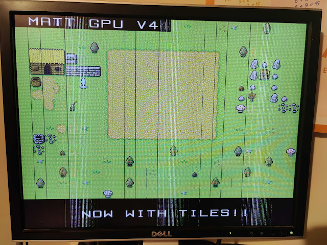
Here's how my tile demo looks:

The colours look nicer because it's a better monitor, but here is a side by side comparison of EEPROM, EPROM and SRAM:

There are still some lines - I'm probably still outside of spec, but I can definitely live with this quality.
I made a demo with some nicer tiles, here is the source:

And the result on my GPU:

I still wanted to benchmark just how much I can do during the vblank. I wanted to try some different libraries but support for the pi 3 isn't as good as the pi 4, so I upgraded to a pi 4.
While I was waiting for the pi 4 to arrive, I added the decoupling caps to all the ICs, because I was getting a little bit of wobble on screen. Adding them seems to have made things a bit better.
When the pi 4 arrived, I implemented some benchmarks to see how many map tiles I could change during vblank.
It can update fast enough, but I noticed some tiles don't update correctly. I think this is due to a flaw in my design, whereby I use the same signal to write to the RAM as I do to enable the data buffer going into the RAM. Ideally these would be separately controllable to avoid any timing issues. I will update that in the final design.
Here is another demonstration of the write problem
The problem is intermittent, so simply writing the same tiles multiple times does fix it, but since I'm pretty sure I know what's causing it, I won't worry about it unless it still occurs with the hardware fix.
To be continued...
The post covers a couple of months of adventures, but due to personal circumstances, I've not been able to spend much more time on it. I plan to finish it as soon as I can, and possibly do a more technical / tutorial style write up, or video, depending on whether people think that would be more useful than this "diary" approach of writing where I'm sometimes quite vague on the details.
The next step is to add the hardware scrolling. It's all working in my emulator, and the schematics have been made - I just need to finish the PCB design and get it fabricated. I hope to get the time and energy to do this soon, at which point I'll make a new post.
Hope you enjoyed the read.


Comments
Post a Comment