BenEater Inspired GPU - Final Design
The final specs
For those of you who want to jump to the details of what it does, here is a summary of the final card
Screen resolution: 400x300
Colours: 256 (RRRGGGBB)
Tile memory: 256 tiles, 16x16 pixels per tile
Map memory: 256x128 tiles (4096x2048 total pixels)
Clock frequency: 20Mhz
VGA mode: 800x600 @60hz
Recap from last time
Last time I had combined the counter board from my first post with a new board responsible for colour output. The new board includes an interface for writing to memory, and also a new memory map. The new memory map contained 2 chips; a tile set and a tile map. The tile set defined an 8 bit colour for each pixel in each tile, and the map defines which tile appears in each "grid space".
The GPU as I left it had enough memory to define a huge map of tiles, but since the screen only outputs 400x300, most of them are useless. The idea is to add hardware scrolling to allow us to "move" the viewport.
Hardware scrolling design
The hardware scrolling is actually incredibly simple to implement. First let's look at how the existing board works.
Currently, the lower 4 bits of the H and V counters select the pixel of the selected tile (16x16 pixels), and the rest of the bits select which tile in the tile map we should be drawing.
In order to "scroll" I simply need to offset H and V. So I implemented 2 registers for H and V (only 12 bits total though), and then run each bit of the counter and the scroll registers through 3x 4 bit adders, which then output the final 'offset' co-ordinate.
Here's the change to the above diagram:
And here is an example of how the tile is selected with an offset of X=10 and Y=0
Super simple!
The reason I have 12 bit maximums for each scroll is because the memory RAM is 256k-bit, which has 15 address lines total. I chose to assign 8 to horizontal and 7 to vertical. Remember we use the lowest 4 bits of H and V to address the pixel within the tile, so that means the maximum binary number H and V can be before we run out of address lines, is 111111111111 and 11111111111 respectively - in other words 4095 and 2047.
I've colour coded the above to show the red bits (underlined for you colour blind people) are used for the tile pixel select, and the remaining green bits are used to select the tile from the map.
This gives us our final possible map size of 256 tiles by 128 tiles (4096 pixels x 2048 pixels)
The new interface protocol
While adding the scroll registers, I had to change the interface a little bit. I wanted to keep the control signals to 8 bits or less, but I needed to be able to:
- Enable drawing
- Disable drawing
- Write to MAR A
- Write to MAR B
- Write to Map
- Write to Tile
- Write to scroll xa
- Write to scroll xb
- Write to scroll ya
- Write to scroll yb
As you can see, I can't have a dedicated line for each of these functions so I made use of multiplexing. I used a 3 input, 8 output demultiplexer IC (74ls138) which makes the interface:
- Write
- Write select A
- Write select B
- Write select C
- Disable drawing
The computer can select the chip to write to via the 3 write select lines:
So for example to scroll the screen 10 pixels to the right:
Another example, set tile at 5,5 on the map to tile index 7
The 'pause' before enabling draw may not be necessary, but will definitely be considered best practice, as the RAM chips technically require the line to finish falling before your data is guaranteed to be written.
In theory since the registers between your DATA input and the RAM IOs are latched on, you should only need to do this before enabling the screen, and not between every operation you do.
Improving the counter
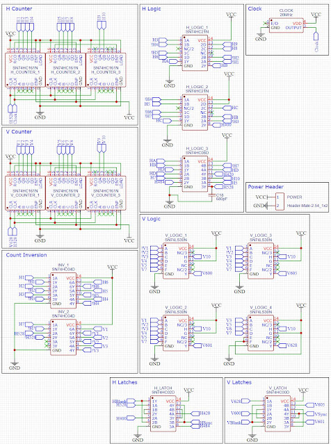
Before diving into the final PCB design, I wanted to pick up the side mission from last time, and improve the counter circuit. The combinational logic in Ben's video is a great way to learn, but it isn't the most efficient strategy. I decided to replace my old 17 chip combinational logic design with the EPROM lookup design. This replaces all the combinational logic used for hsync, vsync, hblank, vblank and counter resets with a single EPROM that is pre-programmed to output the same thing the combinational logic would for every input possible. I found a 20 address line EPROM which would be perfect for the job. The only extra thing it needs is a D flip-flop to smooth out the EPROM outputs, which can change erratically when switching
Schematic before:
Schematic after:
Besides the simple breadboard prototype of just the H count I made, this is pretty much untested, so hopefully it works first time (foreshadowing...)
I couldn't face prototyping the counter logic for the millionth time, so decided to take the risk (not smart...)
Physical interface
This GPU is designed to be standalone, and be driven by an external computer. Whether that's a Raspberry pi, Arduino, 6502, or a homebrew - it doesn't matter.
I had to decide which physical connector I was going to use. The GPU now only requires 5 lines to control it, 8 lines to send data in, and 5v / ground. 15 lines total.
I could have gone for simple header pins, but I've been curious about edge connectors and wanted to have a go at that. After researching different ones, I decided it would be cool if I used the PCI-E form factor. I only needed a tiny little PCI-E x1 to fit all the lines on, but it looked ridiculous compared to the size of the board, so I went for a full on PCI-E x16 connector, because it looks cool and would add physical stability.
I'm only using a fraction of the pins, and am in no way at all following anything like the PCI-E standard, so if anyone plugged this into a PC it will no doubt cause a lot of damage - but it looks pretty rad in my opinion
I also tried to plan the physical dimensions to fit into a standard PC case, even placing the VGA header to hopefully be able to fit a metal bracket to it, which I found on ebay
PCB design
This thing is becoming a bit of a monster in terms of size, number of connections, and number of ICs. The chip count stands at 34 (81 components total including bypass caps), with 184 different 'nets'. The only way I could fit it all on while maintaining physical dimensions as described above, was to make it roughly the size of an NVidia GTX 1080! Of course I could switch to SMC and make it more compact, but I'm not ready for that; learning how to properly solder SMCs will just decrease my chances of actually finishing something!
Even at it's mammoth board size, auto routing was not an option. I tried auto routing with a 4 layer board, but the auto router gave up. I had to painstakingly route every trace by hand. After several iterations of placing the ICs, I eventually came up with an arrangement which would allow me to bus the main parts around together. I drew a little sketch of the rough idea
After quite a few hours of on and off work, I completed all the traces by hand, and even managed to do it on a 2 layer board
A new hat
To test it out, I was going to hook it up to the Raspberry pi as before. The board no longer has any pin headers (except for an emergency 5v/ground header in case my edge connector totally fails, in which case I can at least hook it up to power and check the new counter logic is working). In order to connect this to something, I need a female end to the PCI-E connector.
I made a super simple and quick PCB which simply connects a PCI-E female header to the raspberry PI GPIO, and has the correct form factor to allow it to be screwed on to the Raspberry Pi (aka, a hat)
I sent both off to JLCPCB to be fabricated
Arrival of the final PCBs
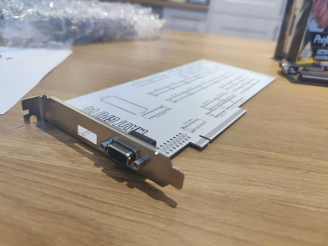
The PCBs arrived and they were a sight to behold!
Here is the size of the thing compared to the old card - it's pretty huge
The bracket I got off Ebay fit too, even though it's pretty pointless, it looks cool, and that's obviously what matters most
Here's the final board with all components in (except bypass caps and the timing ROM)
Here is the board attached via my little pi hat to a raspberry pi. Absolutely ludicrous looking, which I love
New VGA signal logic (fail)
Excitedly I plugged it in and, of course, it didn't work :)
Turns out the (untested, yes I'm an idiot) timing ROM chip just wasn't fast enough to change addresses and output clean signals. I believe the ROM chip I did the proof of concept test with was fast enough, but since this one is bigger, and a totally different, slower chip, it wasn't playing ball.
Below you can see it does correctly send the various signals (hsync, vsync etc) high and low, but between address switches it briefly goes high
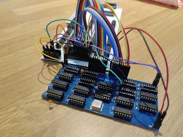
As disheartening as this was, I wasn't about to let this stop me. Once again my old counter board came to the rescue. I simply frankensteined it together with the new board, by feeding the H and V count signals to the counter board, then feeding the sync, blank and counter reset signals from the counter board back to the main board.
In essence the timing ROM chip is just being replaced (or reverted) with combinational logic as per the original design.
It's ugly, but I was determined to get this ridiculous thing working. I plugged it in and... success!
Talking to the GPU
Now I just needed to write some python code for the pi to interface with the card and draw something.
I wrote some simple tests and, the GPU was just ignoring my instructions...
I probed around to see where the fault was, and eventually found the demultiplexing of the instructions wasn't working.
I took a closer look at my schematic and the datasheet for the demultiplexer; see if you can spot the issue:
In my schematic I was assuming E1 was active high, and E2 & E3 were active low. However if you check the pin numbers, E3 is the active high enable and E1 & E2 are the active low enables.
I could correct the signal going to E1 in software, and just require a low signal to enable the demultiplexor instead of a high, however since the active high E3 pin was always tied low, I had to do some hacking.
I bent up one of the ICs little legs, and croc clipped it to 5V
The GPU was now listening to my instructions, and all of it's functions were now working, including scrolling
And here is the tile demo from before with scrolling
The flickering lines is because I'm not waiting for vblank to scroll in this demo
What have I achieved?
On the one hand, after all this effort I'm left with an ugly hacked together GPU, where the only improvement on the last prototype is that it now has scrolling. But on the other hand, I got to try out edge connectors, learned not to bother with the signal ROM hack and just stick to what works (this project is not about efficiency, it's about getting something working and having fun doing it), and finally learned to not make assumptions about schematic diagrams - I think it's about the 10th time I've learned to read the bloody datasheets!
It works though - and it can be hooked up to any computer. It's a nifty little card with it's own simple interface, which then handles all of the logistics of putting pixels on screen for you. It requires an 8 bit data bus hooked up to it, and 5 control lines. It would be very easily hooked up to BenEaters 6502 computer project - so that's exactly what I'm going to do next!
I'm actually quite far into that right now, so the next update should come quite soon
Thanks for reading, I hope this helps someone avoid some of my mistakes - or is at least entertaining to follow the journey of a complete novice fumbling around with electronics.


Comments
Post a Comment